Today’s breakdown is authored by “Lithos Graphien,” an anonymous contributor with decades of experience in the chip industry. Special thanks to Arrian Ebrahimi of Chip Capitols for his edits.
Jordan is in LA next week and holding a meetup! Register here.
We also just published an emergency podcast on the AI executive order. Transcript soon, for now check out the podcast. Here’s the Apple Podcasts link.
The United States and its allies are engaged in a technology cold war against China to block semiconductor computing capabilities used in artificial intelligence and military applications. In recent years, the US Commerce Department has applied a series of export restrictions to achieve just that — and yet, just a few weeks ago, Huawei shocked the world with advanced chip technology that those restrictions were intended to prevent.
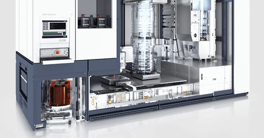
A nation’s computing capabilities are directly related to a complex printing process called semiconductor lithography. Semiconductor factories — called fabs — build microchips by printing layers upon silicon wafer substrates. Scanners — the machines used to print these layers — expose a master image of the circuit pattern onto the substrate until an entire wafer has a grid of patterned chips.
This article dives into the little-known tricks of the lithography trade to understand how the process works behind the scenes. Armed with this insider knowledge, we will then explore:
The technical misunderstandings in prior export regulations between Commerce Department officials and lithographers,
The circumventions that resulted from these misunderstandings,
And whether Commerce’s latest export controls resolved those past loopholes.

Lost in Translation, 2019 to 2022
Generational improvements in scanners have enabled ever finer patterns to be printed on silicon wafers; the shorter the wavelengths, the more accurate the designs. The latest improvements came in the form of immersion scanners and EUV (extreme ultraviolet) scanners.
Immersion scanners use argon fluorine excimer lasers to produce light at a wavelength of 193 nanometers.
EUV scanners are yet more complex: they use a carbon dioxide drive laser to strike a tin droplet which then creates plasma-emitting light at a wavelength of 13.5 nanometers.
US national security leaders are concerned with China’s access to these latest two innovations.
Scanner Process Misunderstanding (2019 Export Controls)
Litho World
Scanners pattern silicon wafers by printing layers of a design — and for decades, the printing process made only a single image per layer. But as step-wise improvements to immersion lithography reached their limits (and before EUV was in the game), chipmakers moved to multi-patterning lithography, a process whereby scanners combine two or more images to make a single layer.
The stacking of layers in a semiconductor device involves two complex verification processes: alignment and overlay.
Pattern alignment is performed by the scanner: it measures the position of a prior image and then exposes a new image upon it.
Overlay is performed by a separate metrology tool after the scanner has completed its work. This measures the final positioning error between the current image and the prior images in the device.
Single-machine overlay (SMO) is the simplest form of this verification. Here, two layers are exposed on the exact same machine to see what the positioning error is. (The error tolerance needed for working microchips is so precise that it’s on the order of single-digit nanometers.) Limiting the verification process to one machine removes the risk of error arising from transferring wafers from one machine to another.
In practice, though, fabs never operate in SMO mode because of logistical realities in high-volume production. Instead, fabs conduct pattern alignment and overlay through matched-machine overlay (MMO). Here, a set of scanners is matched, and a wafer can run through any combination in the matched set. MMO allows for far greater operation flexibility in a fab, but at the cost of nearly doubling the overlay error. Process engineers attempt to reduce the MMO error rate by reducing “runpath combinations” (the number of different machines a wafer runs through), but this strategy works only to a limited extent.
All modern overlay strategies rely on maximizing the accuracy verification (metrology) of both the scanner and overlay tools used to overlap the layers. But metrology is massively expensive: additional alignment measurements require more scanners. Likewise, if the overlay tool required additional metrology, the fab would need a larger fleet of tools to make up for the capacity shortfall. With an eight-figure price tag on these tools, it’s just not affordable to increase metrology indefinitely.
Another important aspect of the litho process which can heavily influence overlay performance is rework. The scanner images a pattern into a temporary organic material called photoresist. This temporary image is then measured to see what the overlay error is; if it’s satisfactory, the image is permanently etched into the device — otherwise, the photoresist is removed, recoated, and reimaged with a dedicated set of corrections. This process always yields the best possible outcome because the exact positions of the pattern are known. In production, the goal is to minimize rework because, for example, if the rework rate were 30%, the fab would need 30% more scanners to make up for the capacity shortfall. In the same way a fab can’t just add metrology due to tool costs, they also can’t demand automatic rework.
To recap, there are three ways to improve overlay performance: reduced runpath combinations such as SMO, increased metrology, and rework. All of these methods are routinely used, but they are also used sparingly in production due to risk or cost reasons.
Department of Commerce
Back in 2019, as TSMC was first releasing their 7nm-node logic ICs, Commerce pressured the Netherlands to impose a ban on China for EUV scanners made by ASML. Its reasoning was that EUV enabled 7nm to be produced at volume scale; indeed, prior to 2019 there was speculation as to whether EUV was going to be ready for the 7nm node. Thus the first iteration of these devices relied on immersion lithography using multi-patterning.
The 7nm node required three to four passes by the scanner to imprint its pattern for a handful of critical layers in the device. That’s the highest number of multi-patterning passes ever attempted with immersion lithography — and a high number of lithography passes plays directly into the production challenge of applying MMO for the 7nm node, and was the rationale for the export rules on immersion scanners that came later (the October 2022 rules, as well as the Netherlands’ June 2023 rules). The introduction of EUV at this node reduced the number of layers needed, and it was under these assumptions that 7nm “at production scale” could be enabled only by EUV. Ultimately, the Netherlands capitulated to this pressure in the same year and banned all EUV scanner exports to China, effectively stopping them at the 10nm node.
Note that the EUV ban covered only logic devices: DRAM (which relies on other methods for each new chip generation) had a ways to go before it would need EUV; NAND Flash, meanwhile, relies on 3D stacking to scale, not shrinking the device geometry, meaning they will never need EUV.
Scanner Measure Misunderstanding (October 2022 Export Controls)
Litho World
In lithography land, you’ll often hear references to words like “resolution,” “half-pitch,” “critical dimension” (CD), or generics like “features” or “geometries.” These all refer to the size of the tiny circuit parts which are printed in each layer. Each microchip generation’s improvement in computational capability relies on shrinking the minimum resolution that can be printed, such that more electronic components can be included. Today’s chips pack an astounding 80 billion transistors into a single exposure field imaged by the scanner.
A scanner’s ability to print smaller geometries is controlled by two aspects of the optical system: the wavelength of light, and the size of the lens. The novel aspect of immersion lithography is that it uses an optical “trick” to make the photoresist think the lens is much bigger than it really is. In the 1800s, scientists figured out that putting water between a microscope lens and the specimen improved visibility. That same concept was used 150 years later for printing chips (hence the name “immersion lithography”).
The resolution of any imaging system with a lens can be defined by way of the Rayleigh criterion: Resolution = k1-factor * wavelength / lens-size.1 Put simply, k1 is a scalar, and it measures how blurry an image is. (In the case of an immersion scanner, the minimum k1 that can be used is 0.27, corresponding to a minimum resolution of 38 nanometers.)
Department of Commerce
The export rules cite the Rayleigh criterion and a specific value for the k1 scaling factor to define what the resolution of an immersion scanner is. That approach is the reverse of how a lithography engineer uses the formula: the minimum geometry (resolution) is fixed on the master pattern, meaning that engineers instead calculate the k1 scalar.
The export rules do the reverse, setting a k1 value that is not even close to 0.27, and then imposing by fiat a k1 value on what the resolution definition for scanners must be — which of course doesn’t represent the real resolution of any system.
Fast forward to October 7, 2022 — Commerce announced a new set of export rules aiming to contain China’s logic capabilities even further, and also attempting to contain memory device performance. The rules require companies to apply for licenses to export the following items to China, effectively cutting off Chinese firms’ access to these chips:
FINFet Logic of 14nm or less (page 108)
DRAM of 18nm or less (page 109)
NAND Flash of 128 layers or more (page 109)
With respect to an immersion scanner: one regulation on resolution restricted the minimum geometry to 45 nanometers or less — and as we discussed above, an immersion scanner can print down to 38 nanometers. The catch is that Commerce inserted a definition for resolution using the Rayleigh criterion, incorrectly setting the k1 factor as 0.35 — meaning that, by their definition, an immersion scanner has a resolution of only 50 nanometers, and was thus not restricted by this rule.
In June 2023, and in coordination with the US Department of Commerce, the Netherlands imposed its own export ban on ASML’s scanners that improved upon what the US had filed. The Dutch rules are as follows:
SMO less than 1.5nm
Resolution less than 45nm @ k1 = 0.25
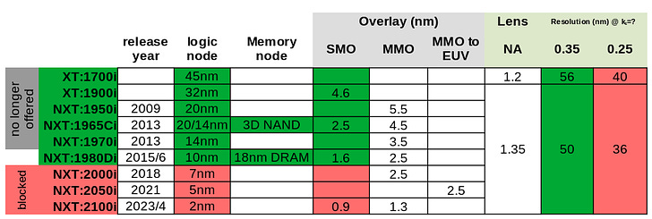
Armed with your short lesson in lithography, you’ll notice right off the bat how these rules also don’t relate to how a fab actually runs. The above table shows updated scanner bans and the corresponding nodes which they are used for. The SMO rule allows the 1980Di scanner, which was used for 10nm logic and 18nm DRAM. And there is no containment for Flash memory by way of any overlay rule. In other words, these rules define the resolution for an immersion scanner beyond what is actually possible. Although on paper that would imply all immersion scanners were banned, this rule was not enforced; these rules were instead interpreted as allowing the 1980Di tools to be exported, but blocking anything newer.
How Misunderstandings Breed Circumventions
It’s clear these rules didn’t work as intended. Allowing Chinese firms to purchase 1980Di scanners doesn’t prevent their ability to produce 14nm logic chips. And as we found out this year, it doesn’t even prevent 7nm logic.
Remember how fabs don’t run in SMO mode, lest a tool goes down and halts production? Well, as it turns out, ASML’s immersion scanners are something of an energizer bunny. They enjoy north of 97% uptime, and can run for months at a time without intervention. But what happens if a tool goes down hard for a long period of time? The Dutch take this lithography business very seriously, and the exorbitant fee that’s paid for the service contract comes with some big benefits. In the event of any catastrophic tool crash, an army of engineers is dispatched within hours and operates on the machine with the choreographed speed and precision far exceeding an Indy 500 pit crew. In other words, the logistical risk of operating in SMO mode for a handful of problematic, multi-patterning layers may not be such a big deal after all.
Remember, SMO has nearly double the performance of the MMO that everyone else operates with. Geometry scaling with multi-patterning is a possibility, as long as the logistical issues are addressed. And recall in our litho lesson that maximizing metrology and automatic rework also improve overlay performance. Further, by slowing down the speed the scanner operates at and increasing the number of alignment measurements, you can play games with how the system works — for instance, to improve the overlay performance enabling multi-patterning at 7nm. Put another way: throwing money at the problem — buying more scanners and overlay tools — is also a solution.
Time will tell if Commerce is right or not about the rule stopping SMIC from producing 7nm “at volume scale.” But so far, allowing ASML’s 1980Di scanner to be sold to China doesn’t block 7nm in the least — and the jury is still out on another leap to 5nm. It’s a similar story with DRAM: nothing prevents those fabs from running with SMO (since they do multi-pattern differently than other fabs), and DRAM companies — like Micron, Samsung, SK hynix, and China’s ChangXin Memory Technologies (CXMT) — won’t need EUV for a number of nodes beyond 18nm DRAM, anyway. Meanwhile, Flash memory wasn’t contained at all: Flash companies — like China’s YMTC — can use any old immersion scanner they want, and nothing stops them from continuing to stack layers on top of each other to expand the memory capacity.
2023 — And Still Lost in Translation
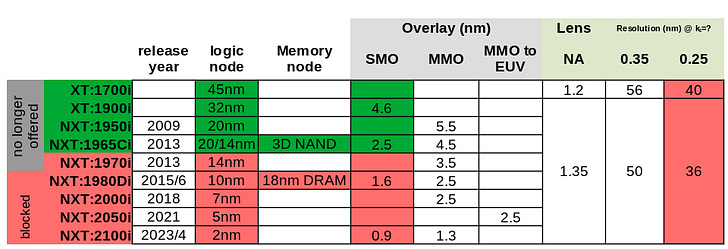
Now we come to the new rules released last week. Seeking to stop Huawei at the 14nm node, Commerce now requires that the following items receive an export license, effectively barring their sale to Chinese companies:
SMO less than 1.5nm (page 17)
SMO less than 2.4nm but greater than 1.5nm (page 17)
Resolution less than 45nm @ k1 = 0.25 (page 30)
Scanner Process Misunderstanding: Plugging One Hole & Poking Open Another
Now we have two rules applied to overlay, further restricting it to 2.5nm. Those rules make a lot of sense: they’re in the spirit of blocking specific logic and memory device nodes. By restricting the SMO to approximately 2.5nm, it now matches where the MMO failed at the 7nm node for multi-patterning. These rules would then allow for only a 1965Ci, blocking everything newer. The result is that a select group of Chinese integrated device manufacturers (IDMs) — SMIC, YMTC, CXMT, and HHGrace/ICRD — are sent a decade back in time.
These rules don’t quite go far enough, however, to block China from making 14nm node logic devices. As we already discussed, there are many overlay tricks that can allow for double patterning (which was used at that node). For DRAM, these rules may very well be successful at stopping CXMT at the 18nm node.
ASML, in their earnings call this week, indicated they are working with Commerce on further clarification, so hopefully that resolves the riddle of these new overlay rules. Would ASML make a new, specially designed product just for the above-mentioned cohort of Chinese IDMs? The answer, from a hardware perspective, would be no — in all likelihood, ASML (and likely Nikon, too) would still be shipping the 1980Di — but the software on the tool would be configured to throttle the overlay performance. In this way, if there were ever a relaxation of the export rules, or if these scanners were sold to another chipmaker, the improved overlay performance could be enabled again.
Scanner Measure Misunderstanding: What Tone Did Commerce Intend to Strike?
On to the resolution mystery: Commerce updated the k1 scaling factor, drastically changing the definition of what the resolution is for an immersion scanner. Remember, this rule was already included in the Dutch export restrictions early in June 2023, but it was never enforced. If Commerce’s referencing this same resolution definition signifies it intends to enforce this rule going forward, the implications are significant: by defining resolution in that way, all immersion scanners violate the rule and would be banned, even the /1700i tool (which has not been produced in over a decade). To be sure, the size of the lens can be varied with the software on the tool and, if needed, could be limited on any tool with a revision. So the minimum resolution could indeed be enforced by ASML on any of these tools from the factory. (If a lithographer were writing a rule with that intent, the rule would simply specify the maximum lens size, avoiding the need to specify the Rayleigh criterion or a specific geometry in a confusing way.)
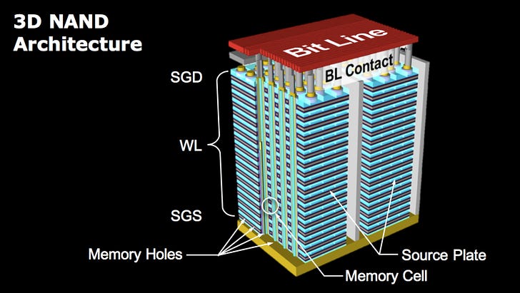
This resolution rule in particular is interesting because of the inability for these export rules to reign in NAND Flash with a simple overlay restriction. Limiting the lens to an aperture size less than 1.1 for a company like YMTC would force its memory capacity to lag something like 20% behind Micron and the others, even if it was keeping up on its stacking expansions into 200+ layers. Such a limitation to an aperture of 1.1 would also be a big disruption to YMTC’s fab operations, as this kind of change would render the master patterns for each layer obsolete and require a complete rebuild from scratch. So again, we need some clarification to see exactly where Commerce was going with this one.
It’s a Wrap
The latest round of export controls is a big improvement with respect to the devices Commerce seeks to prevent a select group of Chinese companies having access to. They likely block 7nm and 10nm node logic, as well as 18nm DRAM. If the resolution rule is enforced for NAND Flash, it will have a huge impact on YMTC’s memory capabilities. These rules, however, likely won’t stop China from producing 14nm node logic, which was part of their intended scope.
You might be wondering, “Are there any other tricks out there that would allow China to circumvent the rules?” Very possibly. For instance, there’s a recent trend in semiconductors that directly addresses the overlay challenge called self-aligned integration, which is a complex series of process steps that make tight overlay control unnecessary. The wide array of tooling needed for these processes spans across much older device nodes and will make enforcement very difficult. With that and other tricks on the horizon, time will tell if China can further outmaneuver these export controls.
An article like this one — where we work together with a deep technical expert to shed light on a core policy question — takes a ton of work to make cogent and legible to a broader audience. If you find this work valuable, please consider supporting ChinaTalk.
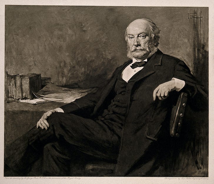
John William Strutt, 3rd Baron Rayleigh, developed this equation back in 1896. He earned a Nobel Prize in physics (in particular, the nature of gasses) — but as kind of a side gig he developed a set of optical equations that describe everything from microscopes, telescopes, and, of course, projection lithography that enabled the digital age.


A few days ago Tom's hardware published an interview with an ex-TSMC exec who believes that the US should concentrate more on maintaining leadership in chip design and not on trying to limit China's progress through trade sanctions. Like the Red Queen said, "If you want to get somewhere else, you must run at least twice as fast as that." If we want to maintain our lead we must out research and out innovate the PRC.
https://www.tomshardware.com/news/us-cannot-halt-chinas-semiconductor-advance-to-5nm-ex-tsmc-vp